

We continuously strive to develop new methodologies for testing and characterisation of metals, alloys and diverse materials such as ceramics, composites, polymers and intermetallics.
Nanosegmentation with Differential Phase Contrast (DPC)
We have developed a rapid, nanoscale image-segmentation technique built on differential phase contrast (DPC) imaging in scanning transmission electron microscopy (STEM). Using a segmented low-angle annular dark-field detector (DF4), we map the projected electric field of the specimen as a false-colour micrograph, in which hue, saturation and value encode the phase, strength and magnitude of the signal. Because different microstructural features — precipitates, clusters, dislocations, grain boundaries — deflect the electron beam in distinct ways, several classes of nanostructure become simultaneously visible and quantifiable within a single field of view, all from a single acquisition taking as little as ~1 minute.
Segmentation is performed by decomposing this hue-saturation-value space: selecting the hue interval associated with a given feature’s phase signature isolates it directly from the DPC micrograph, without separate diffraction or compositional measurements. Compositionally distinct features such as clusters and precipitates produce a different projected potential to the matrix, while dislocations — lacking any chemical contrast — instead generate a phase shift through rotation of the diffraction pattern around their core. This allows precipitates as small as ~2 nm, alongside strain fields and dislocation networks, to be resolved and measured side by side.
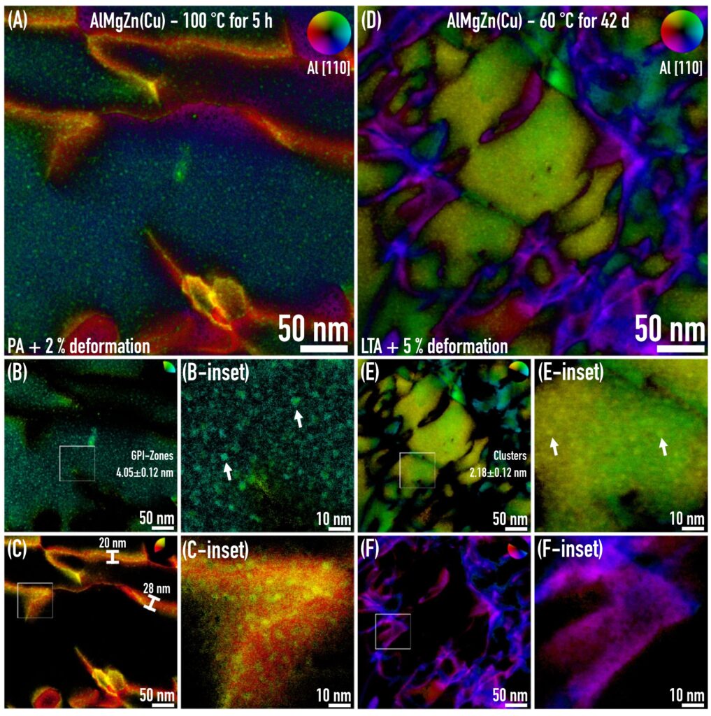
The method is fast, acquiring a full DPC micrograph in 10-30 seconds at 2k resolution, and is readily transferable to any polycrystalline, multi-phase material system.
We have also coupled it with a trained U-Net neural network to automate grain-boundary detection and ASTM E112-compliant grain-size statistics in nanocrystalline thin films.
Software:
HSV-Wizard (Our DPC segmentation app): github.com/SeSam-MUL/HSV-Wizard
SAM-based ASTM grain size analysis: github.com/bnsreenu/python_for_microscopists
Segment Every Grain: github.com/zsylvester/segmenteverygrain
Link for the study:
M. A. Tunes, M. Hasenburger et al. “Unlocking Nanoscale Microstructural Detail in Aluminum Alloys Through Differential Phase Contrast Segmentation in STEM,” Small Methods, 2026, e70743. DOI: 10.1002/smtd.70743
Radiation Damage in Plasma Focused Ion Beam (pFIB)
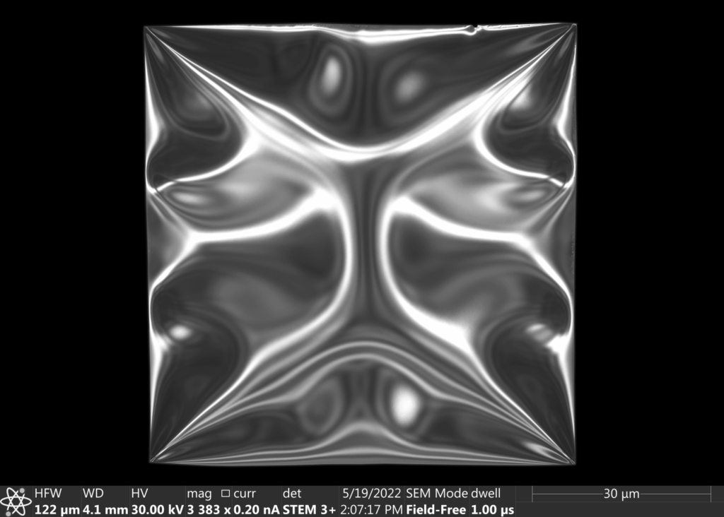
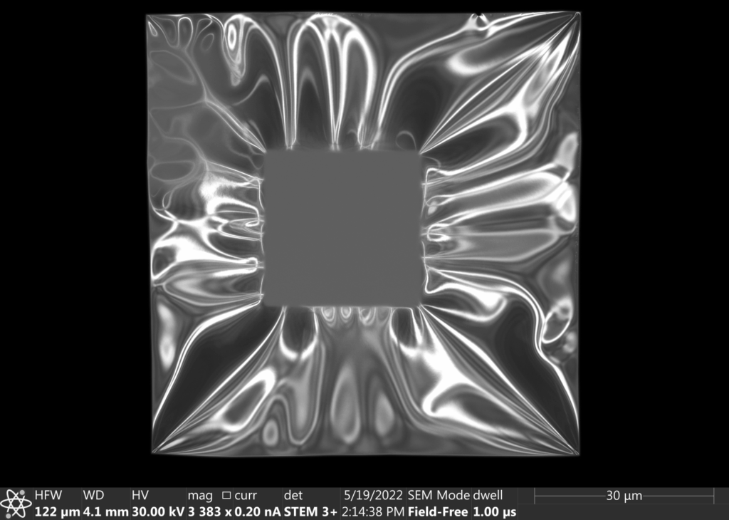
We discovered that the pFIB is a novel platform for investigating radiation effects in materials!
Unlike traditional ion irradiation irradiation methods with limited control and accuracy, the pFIB enables site-specific exposure of a single specimen to multiple doses with exceptional flux stability (±1%) and significantly higher dose rates.
Using ion-beam-induced amorphization in single-crystal silicon as a model system, our technique reveals nanoscale contrast differences between crystalline and amorphous phases, offering new insights into irradiation-induced transformations.
The method opens exciting avenues for research in nanostructuring, device fabrication, and materials under extreme conditions.
Sample preparation for in situ TEM MEMS experiments
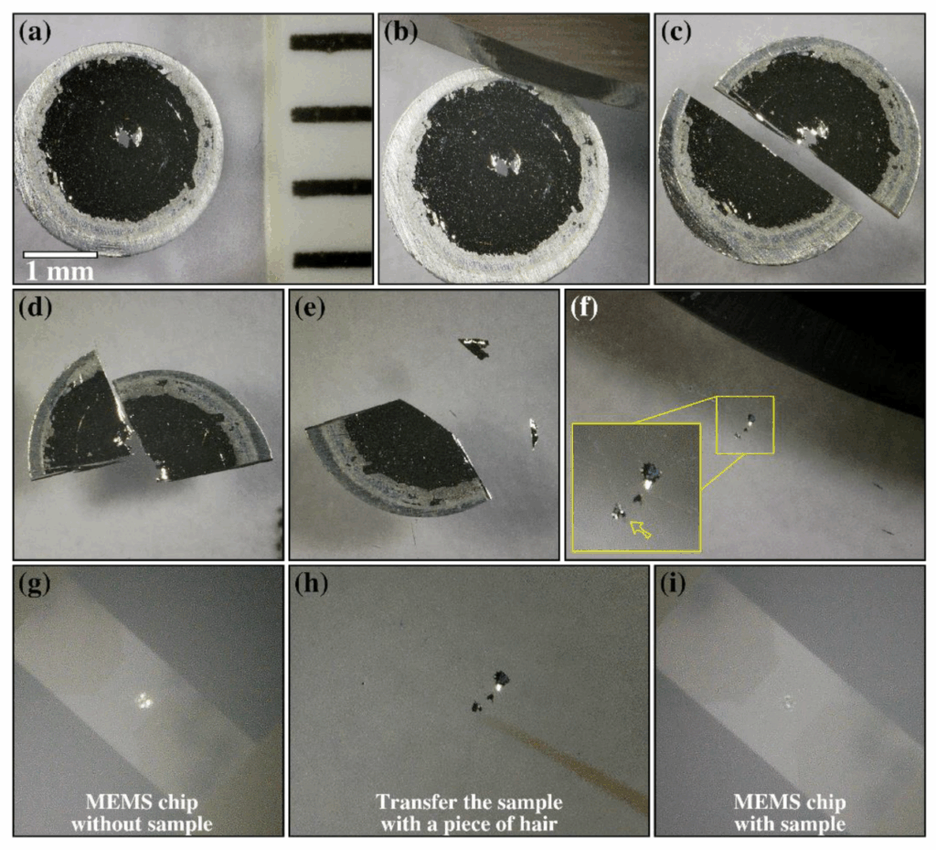
Microelectromechanical systems (MEMS) enable cutting-edge in situ experiments on materials at the nanoscale under extreme conditions, such as rapid heating or complex electrochemical environments. A key challenge, however, lies in preparing clean, electron-transparent samples for MEMS e-chips. We invented a new fast and relatively simple preparation method that minimises contamination (often incurred with the use of Ga FIBs), ensuring reliable experimental conditions. The approach is validated through in situ heat treatment of a crossover AlMgZn(Cu) alloy, demonstrating excellent sample quality and performance within the electron microscope.
Nanometallurgy and nanomaterials
The emergence of nanometallurgy marks a fundamental shift in how materials are tested and understood, driven by the increasing demand for miniaturised devices and the limitations of classical metallurgical concepts at the nanoscale. This new approach redefines materials behaviour by exploring phenomena that are absent or negligible in bulk systems.
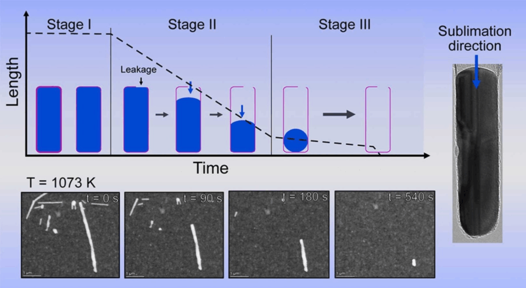
A case in point is the in situ investigation of copper nanowires with diameters between 40 and 140 nm, heated under low-pressure conditions within a TEM. This method enables direct observation of nanoscale processes, revealing significant shape and volume changes with increasing temperature. Sublimation was identified as the dominant mechanism, occurring not only at high temperatures above ≈1023 K, where vapour pressure becomes critical, but also unexpectedly at 923 K, driven by local curvature and atomistic imbalance at the nanowire tips. These insights underscore how nanometallurgy enables the study of size-dependent behaviour under realistic thermal and environmental conditions, offering a powerful framework for developing future materials tailored for extreme miniaturisation.
Ion irradiation/implantation with in situ TEM
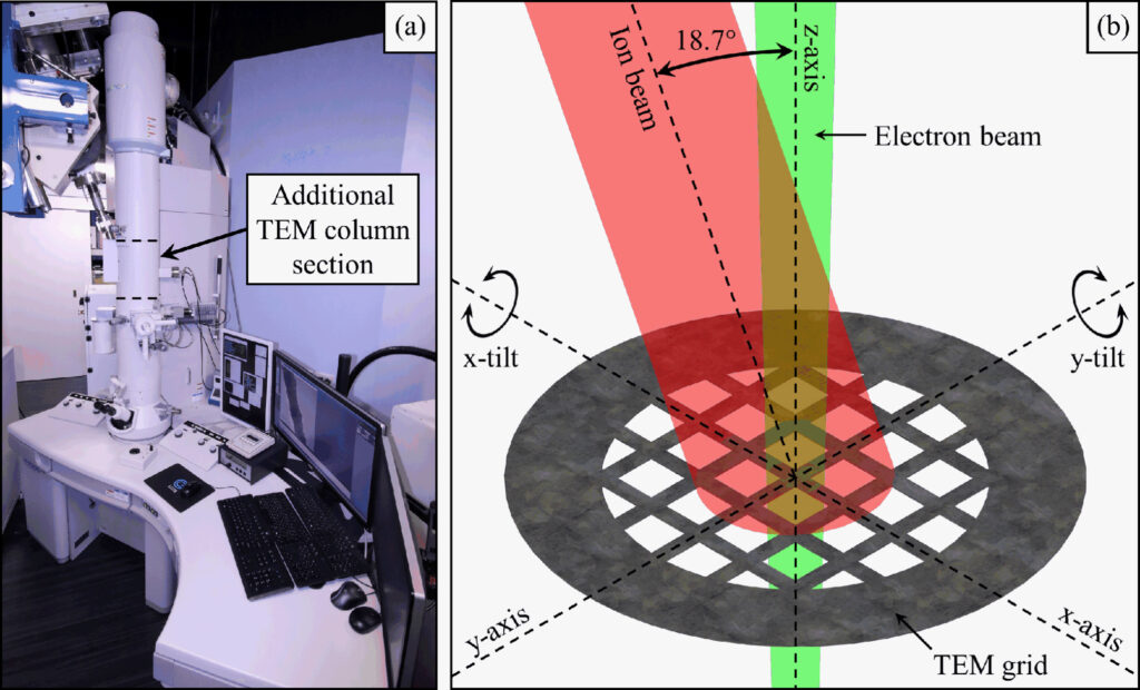
Radiation damage involves complex atomic processes that shape a material’s final structure. The new MIAMI-2 system at the United Kingdom Atomic Energy Authority enables direct observation of these effects using in situ ion irradiation within a 300 kV TEM. It features both medium-energy (350 kV) and low-energy (20 kV) ion beamlines, allowing experiments with a wide range of elements, including dual-ion irradiation with H and He. Operating across a broad temperature range (–170 °C to 1300 °C) and compatible with controlled gas environments, MIAMI-2 offers advanced imaging and analysis capabilities, making it a versatile platform for studying radiation effects in materials for nuclear, semiconductor, and space applications.
More information on the MIAMI Facilities
(a.k.a Jean-Luc Piccard and/or Professor Charles Francis Xavier)